Ge MOSFET
High-mobility Ge is one of the most promising channel materials for future deeply-scalded MOSFETs.
A high quality Ge MOS interface is a key issue for the Ge MOSFETs. We have recently found GeO2/Ge interface formed by thermal oxidation at high temperature exhibited the lowest interface state density among a variety of Ge MOS interfaces [1]. We have evaluated the MOS interface properties by the low temperature conductance method, and the interface state density of less than 1011 cm-2 eV-1 was obtained. The GeO2/Ge p-MOSFET was also demonstrated with the 3x higher hole mobility than Si [2]. We have also successfully demonstrated high performance Ge n-MOSFETs with n+S/D formed by the gas phase doping [3]. We have also investigated ECR plasma post oxidation after for EOT scaling of the Ge MOS gate stack. The high-quality Ge MOS interface with EOT of 0.76 nm has been successfully demonstrated by the post plasma oxidation. The high-performance Ge CMOS with EOT of 0.76 nm have also been successfully demonstrated [4-7].
The Ge condensation and wafer bonding technique has also been investigated for forming Ge-on-Insulator (GOI) and SiGe-on-Insulator (SGOI) integrated on Si wafers [8-10]. (100) and (110) GOI MOSFETs were successfully demonstrated.
By using the direct wafer bonding, the III-V/Ge CMOS structure was demonstrated for the first time [11].
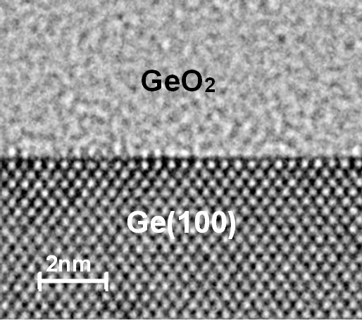
TEM image of GeO2/Ge MOS interface
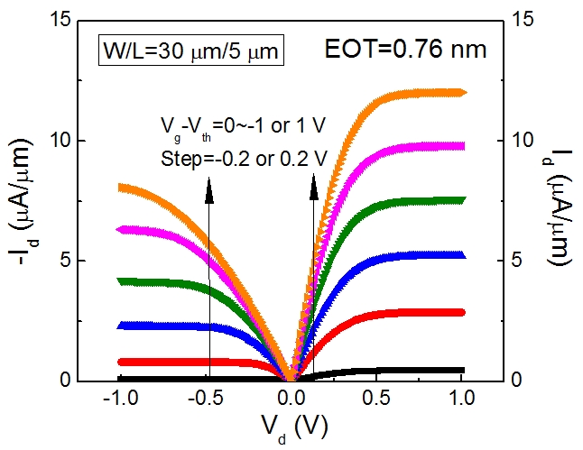
Output characteristics of Ge CMOS formed by plasma post oxidation
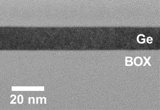
Ge condensation by thermal oxidation
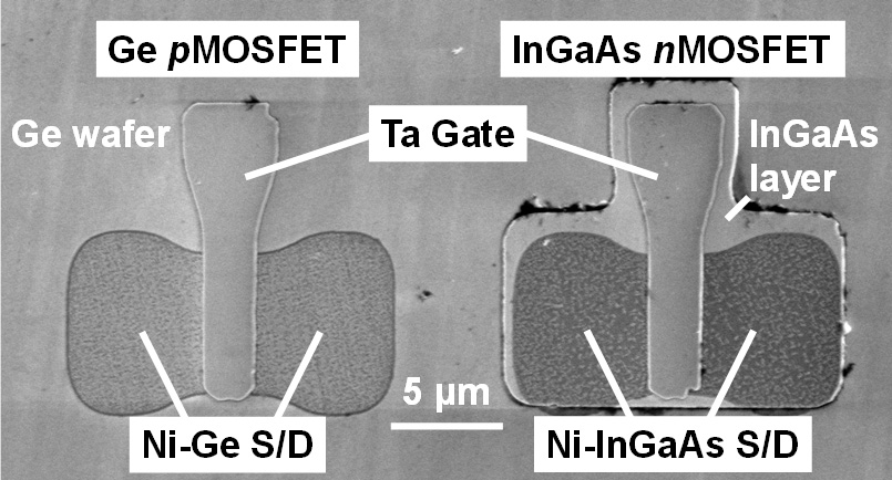
III-V/Ge CMOS
[1] H. Matsubara, T. Sasada, M. Takenaka and S. Takagi, Appl. Phys. Lett., Vol. 93, 032104, 2008.
[2] Y. Nakakita, R. Nakane, T. Sasada, H. Matsubara, M. Takenaka and S. Takagi, International Electron Devices Meeting (IEDM’08), 35-6, San Francisco, December 2008.
[3] K. Morii, T. Iwasaki, R. Nakane, M. Takenaka, and S. Takagi, International Electron Devices Meeting (IEDM’09), 29.3, Baltimore, December 2009.
[4] R. Zhang, N. Taoka, P. Huang, M. Takenaka, S. Takagi, International Electron Devices Meeting (IEDM’11), 28.3, Washington D.C., December 2011.
[5] R. Zhang, P.C. Huang, J.C. Lin, M. Takenaka, S. Takagi, International Electron Devices Meeting (IEDM’12), 16.1, San Francisco, December 2012.
[6] R. Zhang, W. Chern, X. Yu, M. Takenaka, J. L. Hoyt, S. Takagi, " High mobility strained-Ge pMOSFETs with 0.7-nm ultrathin EOT using plasma post oxidation HfO2/Al2O3/GeOx gate stacks and strain modulation," International Electron Devices Meeting (IEDM’13), 26.1, Washington D. C., 11 December 2013.
[7] R. Zhang, X. Yu, M. Takenaka, and Shinichi Takagi, “Impact of channel orientation on electrical properties of Ge p- and n-MOSFETs with 1-nm EOT Al2O3/GeOx/Ge gate stacks fabricated by plasma post oxidation,” IEEE Trans. Electron Devices, vol. 61, no. 11, pp. 3668 – 3675, 2014.
[8] S. Dissanayake, Y. Zhao, S. Sugahara, M. Takenaka, and S. Takagi, J. Appl. Phys., vol. 109, 033709, 2011.
[9] J. Suh, R. Nakane, N. Taoka, M. Takenaka, and S. Takagi, Appl. Phys. Lett., Vol. 99, 142108, 2011.
[10] W. Kim, K. Kuroda, M. Takenaka, and S. Takagi, “Sb-doped S/D ultra-thin body Ge-on insulator nMOSFET fabricated by improved Ge condensation process,” IEEE Trans. Electron Devices, vol. 61, no. 10, pp. 3379 – 3385, 2014.
[11] M. Yokoyama, S. Kim, R. Zhang, N. Taoka, Y. Urabe, T. Maeda, H. Takagi, T. Yasuda, H. Yamada, O. Ichikawa, N. Fukuhara, M. Hata, M. Sugiyama, Y. Nakano, M. Takenaka, and S. Takagi, “III–V/Ge high mobility channel integration of InGaAs n-channel and Ge p-channel metal–oxide–semiconductor field-effect transistors with self-aligned Ni-based metal source/drain using direct wafer bonding,” Appl. Phys. Express., Vol. 5, 076501, 2012.
III-V MOSFET
III-V semiconductors have attracted attention as candidates of high performance n-MOSFETs because of their high intrinsic electron mobilities and low effective masses.
In order to integrate the III-V materials with the conventional Si platform, we are conducting the research on the direct wafer bonding technology[1-2]. The III-V-on-Insulator (III-V-OI) on Si wafer has been successfully obtained by bonding an InGaAs/InP wafer to an SiO2/Si wafer. We have obtained extremely-thin-body 3-nm-thick InGaAs layer on Si by wafer bonding and well-behaved MOSFET operation [3].
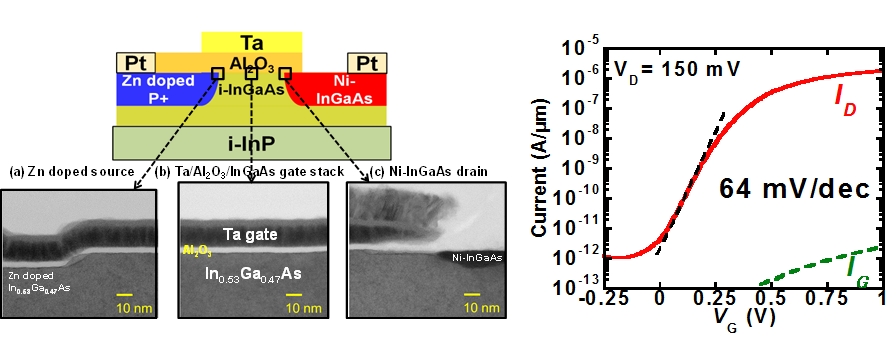
Metal S/D technology has also been investigated, which enables self-align low-resistance S/D with low temperature instead of conventional ion implantation [4-5]. We have found that Ni-InGaAs alloy can be obtained by direct reaction of Ni and InGaAs, which suitable for self-align metal S/D for InGaAs MOSFETs. We have successfully demonstrated deeply-scaled metal S/D InGaAs MOSFETs with 55-nm gate length fabricated on III-V-OI on Si wafer [6].The 20-nm-gate-length InGaAs FINFET has also been demonstrated [7].
InGaAs MOS interface has also been investigated by using atomic layer deposition (ALD). We found that the HfO2/InGaAs MOS interface properties was strongly dependent on the deposition temperature of HfO2. The HfO2/InGaAs MOS interface with 200 ℃ deposition exhibited lowest interface trap density[7]. We have also found that interfacial layer of 2-cycle Al2O3 between HfO2 and InGaAs improved the interface properties, and MOS interface with CET of 1.08 nm has been successfully demonstrated[8]. The interface traps inside the conduction band of InGaAs have also been investigated. We have clarified that the interface traps inside the conduction band affected the transistor performances by using Hall measurements and C-V measurements[9].
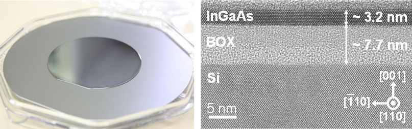
III-V-on-insulator wafer bonded on Si
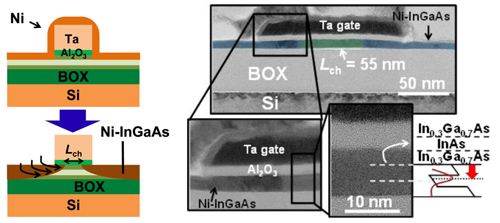
Self-align Ni-InGaAs metal S/D for Ni-InGaAs MOSFETs
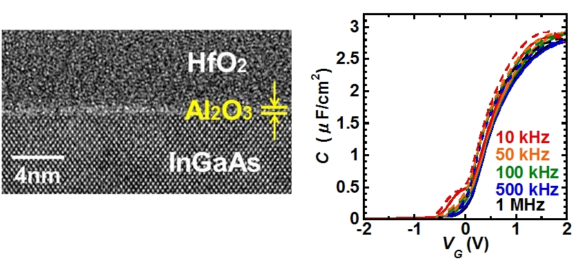
TEM image and C-V characteristic of HfO2/Al2O3/InGaAs MOS capacitor with CET of 1.08 nm
[1] M. Yokoyama, T. Yasuda, H. Takagi, H. Yamada, N. Fukuhara, M. Hata, M. Sugiyama, Y. Nakano, M. Takenaka, and S. Takagi, VLSI Symposium., 12B-3, Kyoto, June 2009.
[2] M. Yokoyama, T. Yasuda, H. Takagi, H. Yamada, N. Fukuhara, M. Hata, M. Sugiyama, Y. Nakano, M. Takenaka, S. Takagi, Appl. Phys. Express., Vol. 2, 124501, 2009.
[3] M. Yokoyama, R. Iida, S. H. Kim, N. Taoka, Y. Urabe, T. Yasuda, H. Takagi, H. Yamada, N. Fukuhara, M. Hata, M. Sugiyama, Y. Nakano, M. Takenaka, and S. Takagi, International Electron Devices Meeting (IEDM’10), 3.1, San Francisco, December 2010.
[4] S.H. Kim, M. Yokoyama, N. Taoka, R. Iida, S. Lee, R. Nakane, Y. Urabe, N. Miyata, T. Yasuda, H. Yamada, N. Fukuhara, M. Hata, M. Takenaka, S. Takagi, International Electron Devices Meeting (IEDM’10), 26.6, San Francisco, December 2010.
[5] S.H. Kim, M. Yokoyama, N. Taoka, R. Nakane, T. Yasuda, M. Ichikawa, N. Fukuhara, M. Hata, M. Takenaka, S. Takagi, International Electron Devices Meeting (IEDM’11), 13.4, Washington D.C., December 2011.
[6] S. H. Kim, M. Yokoyama, N. Taoka, R. Nakane, T. Yasuda, O. Ichikawa, N. Fukuhara, M. Hata, M. Takenaka, S. Takagi, VLSI Symposium., 21.1, Honolulu, June 2012.
[7] S. H. Kim, M. Yokoyama, R. Nakane, M. Ichikawa, T. Osada, M. Hata, M. Takenaka, S. Takagi, "High performance sub-20-nm-channel-length extremely-thin body InAs-on-Insulator tri-gate MOSFETs with high short channel effect immunity and Vth tunability," International Electron Devices Meeting (IEDM’13), 16.4, Washington D. C., 10 December 2013.
[8] R. Suzuki, Noriyuki Taoka,M. Yokoyama,S.H. Kim, T. Hoshii,T. Maeda,T. Yasuda,O. Ichikawa, N. Fukuhara, M. Hata, M. Takenaka, and S. Takagi, J. Appl. Phys., vol. 112, 084103, 2012.
[9] R. Suzuki, N. Taoka, M. Yokoyama, S. Lee, S. H. Kim, T. Hoshii, T. Yasuda, W. Jevasuwan, T. Maeda, O. Ichikawa, N. Fukuhara, M. Hata, M. Takenaka, and S. Takagi, Appl. Phys. Lett., Vol. 100, 132906, 2012.
[10] N. Taoka, M. Yokoyama, S.H. Kim, R. Suzuki, R. Iida, S. Lee, T. Hoshii, W. Jevasuwan, T. Maeda, T. Yasuda, O. Ichikawa, N. Fukuhara, M. Hata, M. Takenaka, and S. Takagi, International Electron Devices Meeting (IEDM’11), 27.2, Washington D.C., December 2011.
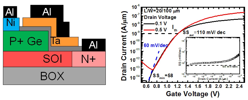
Tunnel FET
It is well known that the theoretical lower limit of S.S. in MOSFETs amounts to 60 mV/dec at room temperature because of the nature of the operation principle of MOSFET This fact leads to an essential limitation of scaled CMOS under future technology nodes especially in terms of driving voltage scaling. Thus, tunneling field-effect transistors (TFETs) have recently stirred a strong interest as one candidate of promising low power switching devices with S.S. lower than 60 mV/dec at room temperature.
We have investigated InGaAs-based tunnel FETs because the higher unneling probability associated with the lower tunneling barrier, the smaller tunneling mass and the direct tunneling properties in InGaAs as compared with Si.
We have successfully demonstrated lateral-pin-structure InGaAs tunnel FETs.
We are currently trying to improve the transistor characteristics of InGaAs tunnel FETs.
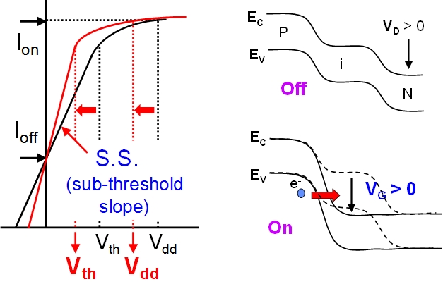
Operation principle of Tunnel FET
InGaAs tunnel FET
Ge/Si tunnel FET
[1] R. Iida, S. H. Kim, M. Yokoyama, N. Taoka, S. H. Lee, M. Takenaka, and S. Takagi, J. Appl. Phys., vol. 110, 124505, 2011.
[2] R. Iida, S. H. Kim, M. Yokoyama, N. Taoka, S. H. Lee, M. Takenaka and S. Takagi, International Conference on Solid State Devices and Materials (SSDM’11), D-4-1, Nagoya, September 2011.
[3] M. Noguchi, S. Kim, M. Yokoyama, O.Ichikawa, T. Osada, M. Hata, M. Takenaka, S. Takagi, International Electron Devices Meeting (IEDM’13), 28.1, Washington D. C., 11 December 2013.
[4] M. Kim, Y. Wakabayashi, R. Nakane, M. Yokoyama, M. Takenaka and S. Takagi, International Electron Devices Meeting (IEDM’14), 13.2, San Francisco, 16 December 2014.
[5] M. Kim, Y. Kim, M. Yokoyama, R. Nakane, S.-H. Kim, M. Takenaka, and S. Takagi, Thin Solid Films, Vol. 557, pp. 298-301, 2014.
[6] M. Kim, Y. Ki. Wakabayashi, M. Yokoyama, R. Nakane, M. Takenaka, and Shinichi Takagi, IEEE Trans. Electron Devices, vol. 62, no. 1, pp. 9 – 15, 2015.
On-chip optical interconnect
The performance of MOSFETs in large-scale integrated circuit (LSI) have been enhanced by the scaling law. However, the power consumption and signal delay in interconnect of LSI has been serious issues, which cannot be resoved by device scaling. To resove the interconnect issues, we have investigated on-chip optical interconnect using Si photonics. Si photonics is the standard platform for large-scale photonic integrated circuits (PICs). We have investigaed the heterogeneous integration of SiGe, Ge, and III-V semiconductors on Si photonics platform for on-chip and off-chip optical interconnects.
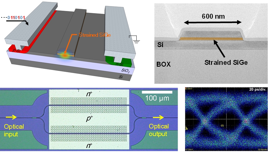
Strained SiGe optical modulator
Si optical modulators are one of the fundamental building for optical interconnections, however the modulation efficiency of Si modulators is poor due to the weak plasma dispersion effect in Si. To overcome this problem, we have proposed to enhanced the free carrier effects by introducing a light-effectice-mass semiconductor on Si photonics platform [1]. We have investigated Si optical modulators with strained SiGe which has a light hole effective mass due to the compressive strain. Owing to the light hole effective mass, we have predicted that strained SiGe exhibits larger plasma dispersion effect than Si [1]. By using carrier-injection SiGe optical modulator, we have successfully demonstrated the enhanced plasma dispersion effect and free-carrier absorption [2-4]. We have also demonstrated 10 Gbps modulation in the Mach-Zehnder interferometer SiGe optical modulator [5]. Since SiGe has been widely used in CMOS fabs, we are now investigating with companies to make real products [6].
Strained SiGe optical modualtor
[1] M. Takenaka and S. Takagi, IEEE J. Quantum Electron., vol. 48, no. 1, pp. 8 - 15, 2012.
[2] Y. Kim, M. Takenaka, T. Osada, M. Hata, S. Takagi, "Strain-induced enhancement of free-carrier effects in SiGe for optical modulator and VOA applications," Optical Fiber Communication Conference (OFC2014), Th1C.4, San Francisco, 13 March 2014.
[3] Y. Kim, M. Takenaka, T. Osada, M. Hata, and S. Takagi, “Strain-induced enhancement of plasma dispersion effect and free-carrier absorption in SiGe optical modulators”, Scientific Reports, vol. 4, 4683, 2014.
[4] Y. Kim, J. Fujikata, S. Takahashi, M. Takenaka, and S. Takagi, "Record-low injection-current strained SiGe variable optical attenuator with optimized lateral PIN junction," European Conference on Optical Communication (ECOC’14), Cannes, P.2.6, 24 September 2014.
[5] Y. Kim, J. Fujikata, S. Takahashi, M. Takenaka, and S. Takagi, "SiGe-based carrier-injection Mach-Zehnder modulator with enhanced plasma dispersion effect in strained SiGe," Optical Fiber Communication Conference (OFC2015), Tu2A.7, Los Angeles, 24 March 2015.
[6] J. Fujikata, M. Noguchi, J. Han, S. Takahashi, M. Takenaka, and T. Nakamura, “Record-high Modulation-efficiency Depletion-type Si-based optical modulator with in-situ B doped strained SiGe layer on Si waveguide for 1.3 um wavelength,” European Conference on Optical Communication (ECOC 2016), Düsseldorf, Tu3.A.4, 20 September 2016.
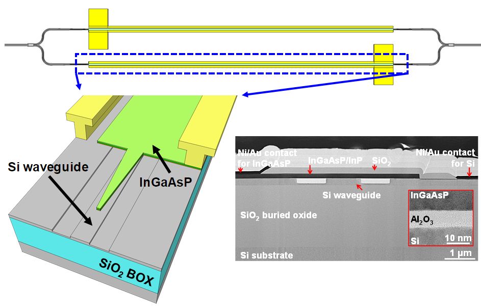
III-V/Si hybrid MOS optical modulator
Since III-V semiconductors have a light electron effectice mass, the electron-induced refractived index change in III-V semiconductors such as InGaAsP is expected to be significantly greater than that in Si. Thus, we have proposed III-V/Si hybrid MOS optical modulator by bonding an n-InGaAsP layer on a Si waveguide with a thin Al2O3 gate dielectric [1-4]. We have successfully achieved optical phase modulation by using accummulated electrons at the InGaAsP MOS interface for the first time. We have achieved an extreamly high modualtion efficiency of 0.047 Vcm, which is one of the highest modulation efficiency among semiconductor-based optical modulators reporeted so far. The optical loss accompanied with optical phase modulation is also reduced by 1/10, enabling high-efficiency, low-loss, and high-speed optical modulators. Now, we are conducting the research of Si optical modualtors beyond 100 Gbps modulation speed.
III-V/Si hybrid MOS optical modulator
[1] J.-H. Han, F. Boeuf, J. Fujikata, S. Takahashi, S. Takagi, and M. Takenaka, “Efficient low-loss InGaAsP/Si hybrid MOS optical modulator,” Nature Photonics, vol. 11, no. 8, pp. 486–490, Jul. 2017.
[2] J. Han, M. Takenaka, and S. Takagi, “Extremely high modulation efficiency III-V/Si hybrid MOS optical modulator fabricated by direct wafer bonding,” International Electron Devices Meeting (IEDM’16), 25.5, San Francisco, 7 December 2016.
[3] J. Han, S. Takagi, and M. Takenaka, “High-Efficiency O-Band Mach-Zehnder modulator based on InGaAsP/Si hybrid MOS capacitor,” Optical Fiber Communication Conference (OFC2017), W3E.2, Los Angeles, 22 March 2017.
[4] J. Han, M. Takenaka, and S. Takagi, “Study on void reduction in direct wafer bonding using Al2O3/HfO2 bonding interface for high-performance Si high-k MOS optical modulators,” Jpn. J. Appl. Phys., Vol. 55, 04EC06, 2016.
Ge photodetector
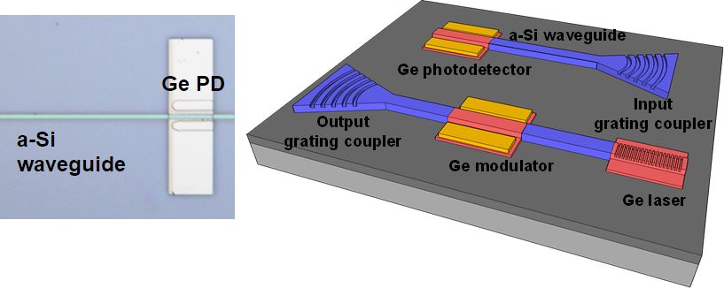
High-sensitivity Ge photodetectors (PDs) has been investigated. One of the critical issues of Ge PDs is large dark current as compared with InGaAs PDs. We have successfully reduced the dark current of the Ge PDs by forming n+/p junction by gas-phase doping [1] instead of ion implantation. In addition, it was found that the GeO2 surface passivation was effective to reduce the surface leakage current[2, 3]. We have also successfully fabricated Ge-on-Insulator wafers by using direct wafer bonding. On the GeOI wafer, we have successfuly demonstrated a waveguide Ge PD monolithically integrated with a-Si passive waveguides [4]. We are now investigating the Ge/a-Si hybrid platform which can integrated Ge/GeSn lasers, Ge modulators, Ge PDs, and a-Si passive waveguides on the GeOI wafer.
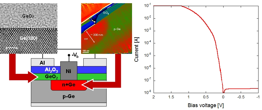
Ultra-low dark current Ge PD
Ge/a-Si hybird platform
[1] M. Takenaka, K. Morii, M. Sugiyama, Y. Nakano, and S. Takagi, Jpn. J. Appl. Phys., Vol. 50, 010105, 2011.
[2] M. Takenaka, K. Morii, M. Sugiyama, Y. Nakano, and S. Takagi, Optics Express Letters, vol. 20, no. 8, pp. 8718-8725, 2012.
[3] J. Kang, R. Zhang, M. Takenaka, and S. Takagi, "Suppression of dark current in GeOx-passivated germanium metal-semiconductor-metal photodetector by plasma post-oxidation," Optics Express, vol. 23, no. 13, pp. 16967-16976, 2015.
[4] J. Kang, M. Takenaka, and S. Takagi, “Ge waveguide photodetector on wafer-bonded Ge-on-insulator substrate monolithically integrated with amorphous Si waveguide,” European Conference on Optical Communication (ECOC 2016), Düsseldorf, W3.F.2, 21 September 2016.
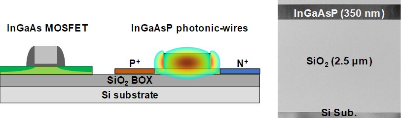
III-V CMOS photonics
We have proposed the III-V CMOS photonics platform on which ultra-small III-V photonics and high-performance III-V transistors can be monolithically integrated [1, 2]. By using III-V-on-Insulator (III-V-O) wafers, which is similar to silicon-on-Insulator (SOI) wafers for Si photonics, we can achieve the strong optical confinement in the III-V-OI, enabling ultra-small III-V photonic devices. The SOI-based waveguide itself does not allow active functionalities, while InP-based photonic wire can achieve active/passive integration, much suitable for ultimately high-performance electronic-photonic integrated circuits (EPIC). We are investigating Si-photonics-like III-V photonics by using the III-V CMOS photonics platform. We have successfully fabricated the III-V-OI wafer on Si by the direct wafer bonding of an InGaAsP/InP wafer and an SiO2/Si wafer [3]. By using the III-V-OI wafer, we have successfully demonstrated an ultra-small bend waveguide, an ultra-small arrayed waveguide grating [3], a grating coupler [4]. We have also demonsrated active devices such as a carrier-injection modulator/switch [4, 5] and waveguide InGaAs PD [6-8]. Moreover, we have successfully achieved monolithic integration of an InGaAsP optical modualtorand an InGaAsP driver MOSFET. Now we are conducting the research for electronic-photonic integrated circuits (EPICs) which can integrate lasers, modualtors, photodetectors, and InGaAs MOSFET on the III-V CMOS photonics platform based on CMOS technologies.
III-V CMOS photonics platform
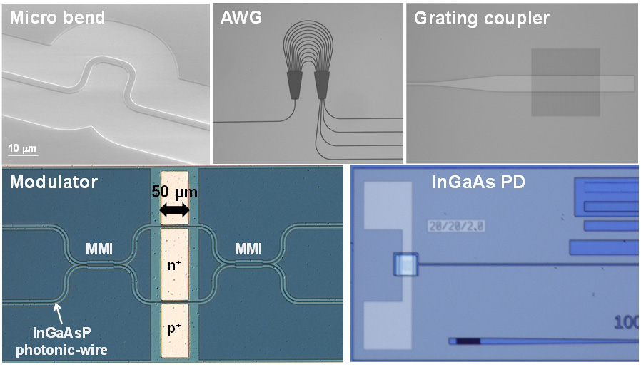
Active and passive devices on III-V CMOS photonics platform
[1] M. Takenaka and Y. Nakano, Optics Express Letters, vol. 15, no. 13, pp. 8422-8427, 2007.
[2] M. Takenaka, M. Yokoyama, M. Sugiyama, Y. Nakano, and S. Takagi, Optical Fiber Communication Conference (OFC’10), OThS5, San Diego, March 2010.
[3] M. Takenaka, M. Yokoyama, M. Sugiyama, Y. Nakano, and S. Takagi, Appl. Phys. Express., Vol. 2, 122201, 2009.
[4] Y. Ikku, M. Yokoyama, O. Ichikawa, M. Hata, M. Takenaka, and S. Takagi, Optics Express Letters, vol. 20, no. 26, pp. B357-B364, 2012.
[5] J.-K. Park, J. Han, M. Takenaka, and S. Takagi, “InGaAsP variable optical attenuator with lateral P-I-N junction formed by Ni-InGaAsP and Zn diffusion on III-V on insulator wafer,” MRS Advances, vol.1 no. 48, pp. 3295-3300, 2016. [6] Y. Cheng, Y. Ikku, M. Takenaka, and S. Takagi, IEICE Electronics Express, vol. 11, no. 16, pp. 20140609, 2014.
[7] Y. Cheng, Y. Ikku, M. Takenaka, and S. Takagi, “Surface leakage reduction in MSM InGaAs photodetector on III–V CMOS photonics platform,” IEEE Photonics Technology Letters, Vol. 27, No. 14, pp. 1569-1572, 2015.
[8] Y. Cheng, Y. Ikku, M. Takenaka, and S. Takagi, “Low-dark-current waveguide InGaAs metal–semiconductor–metal photodetector monolithically integrated with InP grating coupler on III–V CMOS photonics platform,” Jpn. J. Appl. Phys., Vol. 55, 04EH01, 2016.
Deep learning based on universal photonic integrated circuits
Owing to the recent development of Si photonic technolgies, universal photonic integrated circuits (PICs) composed of meshed Mazh-Zehnder interferometer switches have gain considerable attention. Universal PICs are able to perform arbitrary linear operations, enabling various functionalties for optical communications, LiDAR, deep learning based on photonic neural network, and quantum computing. It is essential for universal PICs to realize high-peformance optical phase shifter on Si PICs. We have successfully demonstrated a Si hybrid MOS optical phase shifter, exhibting 1000 times faster switching speed and 1 million smaller power cosumption than a thermo-optic optical phase shifter [1, 2]. By using a Si hybrid MOS optical phase shifter, we can enhance the performance of a universal PIC significantly. We have conducted research of deep learning using universal PICs with Si hybrid MOS optical phase shifter [3].
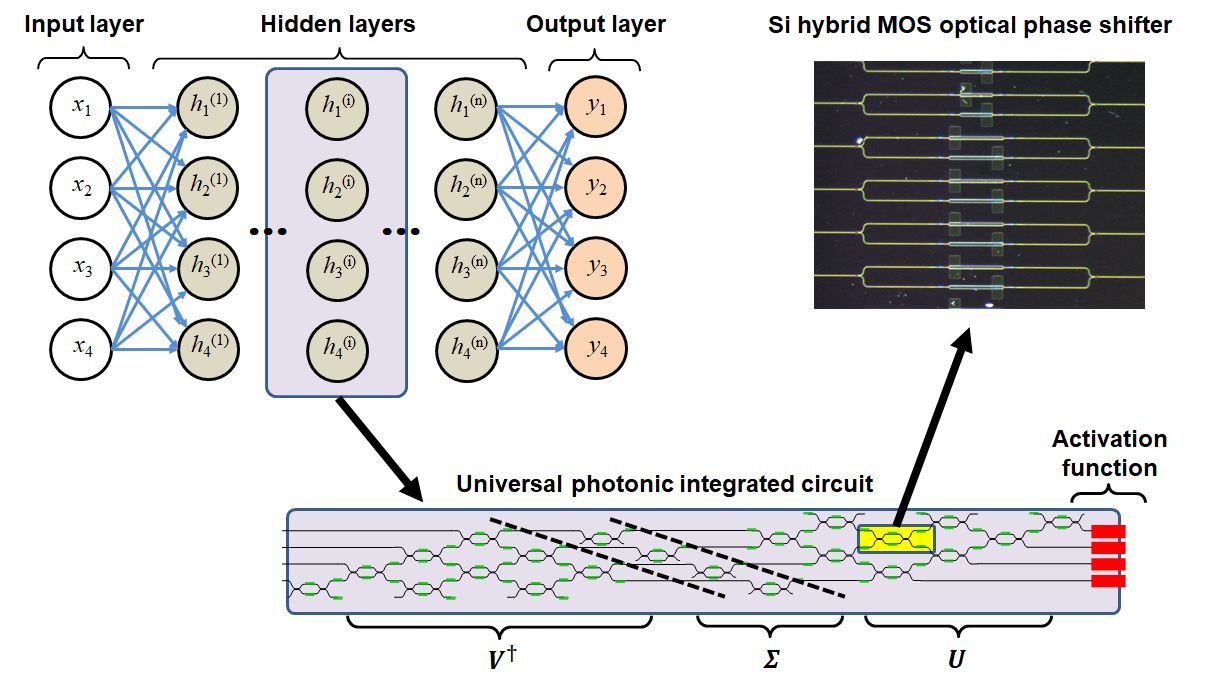
Deep learning using universal photonic integrated circuits with III-V/Si hybrid MOS optical phase shifters
[1] J.-H. Han, F. Boeuf, J. Fujikata, S. Takahashi, S. Takagi, and M. Takenaka, “Efficient low-loss InGaAsP/Si hybrid MOS optical modulator,” Nature Photonics, vol. 11, no. 8, pp. 486–490, Jul. 2017.
[2] Q. Li, J.-H. Han, C. Ho, S. Takagi, and M. Takenaka, “Low-crosstalk, low-power Mach-Zehnder interferometer optical switch based on III-V/Si hybrid MOS phase shifter,” Optical Fiber Communication Conference (OFC2018), Th3C.5, San Diego, 15 March 2018.
[3] M. Takenaka, J.-H. Han, J.-K. Park, F. Boeuf, J. Fujikata, S. Takahashi, and S. Takagi, “High-efficiency, low-loss optical phase modulator based on III-V/Si hybrid MOS capacitor,” Optical Fiber Communication Conference (OFC2018), March 2018 (invited).
MIR photonic integrated circuits
Recently mid-infrared (MIR) photonic integrated circuits (PICs) has gain considerable attention for fiber/free-space optical communication and optical sensing applications. Since many molecules have strong optical absorption in MIR wavelengths from 2 um to 15 um associated with molecular vibrations, MIR photonics is particularly promising for bio-medical sensors, gas sensors, and environmental monitors. Compared to near infrared light for optical fiber communication, MIR light has not been fully utilized because of the technology issues. However, the recent development of Si photonics enables Si MIR PICs. Due to the absorption of Si, Si MIR PICs cannot operation beyond 7 um wavelenth. To overcome this problem, we have investigated Ge-based MIR PICs which can operation at the entire MIR spectrum. We have proposed the Ge CMOS photonics platform which can integrate Ge MIR waveguides and Ge CMOS on Ge-on-Insulator (GeOI) wafer [1-4]. We have successfully fabricated high-quality GeOI wafer using wafer bonding. Thus, various Ge passive waveguides such as micro bends, MMI couplers, ring resonators, grating couplers, photonic crystal cavities have been demonstrated on the GeOI wafer. We have also demonsrated carrier-injection Ge optical modulator operation at MIR wavelength for the first time. Now we are exploring the new frontier of Ge MIR PICs for sensing and optical communication.
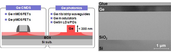
Ge CMOS photonics platform
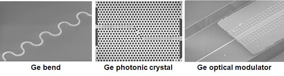
Ge active and passive devices
[1] J. Kang, X. Yu, M. Takenaka and S. Takagi, “Impact of thermal annealing on Ge-on-Insulator substrate fabricated by wafer bonding,” Materials Science in Semiconductor Processing, vol. 42, Part 2, pp. 259-263, 2016.
[2] J. Kang, M. Takenaka, and S. Takagi, “Novel Ge waveguide platform on Ge-on-insulator wafer for mid-infrared photonic integrated circuits,” Optics Express, vol. 24, no. 11, pp. 11855-11864, 2016.
[3] J. Kang, Z. Cheng, W. Zhou, T.-H. Xiao, K.-L. Gopalakrisna, M. Takenaka, H. K. Tsang, and K. Goda, “Focusing subwavelength grating coupler for mid-infrared suspended membrane germanium waveguides,” Optics Letters, vol. 42, no. 11, pp. 2094 – 2097, 2017.
[4] T. H. Xiao, Z. Zhao, W. Zhou, M. Takenaka, H. K. Tsang, Z. Cheng, and K. Goda, “Mid-infrared germanium photonic crystal cavity,” Optics Letters, vol. 42, no. 15, pp. 2882 – 2885, 2017.
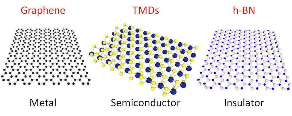
2D material devices
After the successful exfoliation of single-layer graphene, 2D materials have been intensively investigated around the world because of thier unique material properties. By using metal-like graphene, semiconducting TMDs such MoS2, and insulating h-BN, various electronic and photonic devices and flexible integrated ciruits have been investigated. We are conducing graphene modulator/photodetector [1, 2] and MoS2 MOSFETs [3].
2D materials
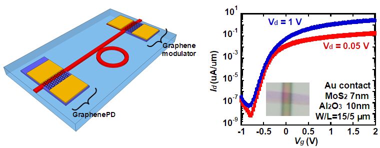
Graphene based photonic devices and MoS2 MOSFET
[1] T. Kayoda, J. Han, M. Takenaka and S. Takagi, "Evaluation of Chemical potential for graphene optical modulators based on the semiconductor-metal transition," International Conference on Group IV Photonics (GFP2013), ThD5, Seoul, 29 August 2013.
[2] Y. Yamaguchi, S. Takagi, and M. Takenaka, “Low-optical-loss graphene-based phase modulator operating at mid-infrared wavelength,” International Conference on Solid State Devices and Materials (SSDM2017), PS-7-03, Sendai, 19-22 September 2017.
[3] M. Takenaka, Y. Ozawa, J. Han, and S. Takagi, “Quantitative evaluation of energy distribution of interface trap density at MoS2 MOS interfaces by the Terman method,” International Electron Devices Meeting (IEDM’16), 5.8, San Francisco, 5 December 2016.