Welcome to TAKAGI and TAKENAKA Group!
New web site for Takagi-Toprasertpong Laboratory is opened (2021/6/1)
New web site for Takenaka laboratory is opened (2021/3/6)

- Dr. Kasidit Toprasertpong has been promoted to Lecturer(2021/6/1)NEW
- Member Updated(2021/4/4) NEW
- Dr. Mitsuru Takenaka is promoted to Professor. NEW
- Member Updated(2020/10/1) NEW
- Publications Updated(2020/5/24)
- Archives ...
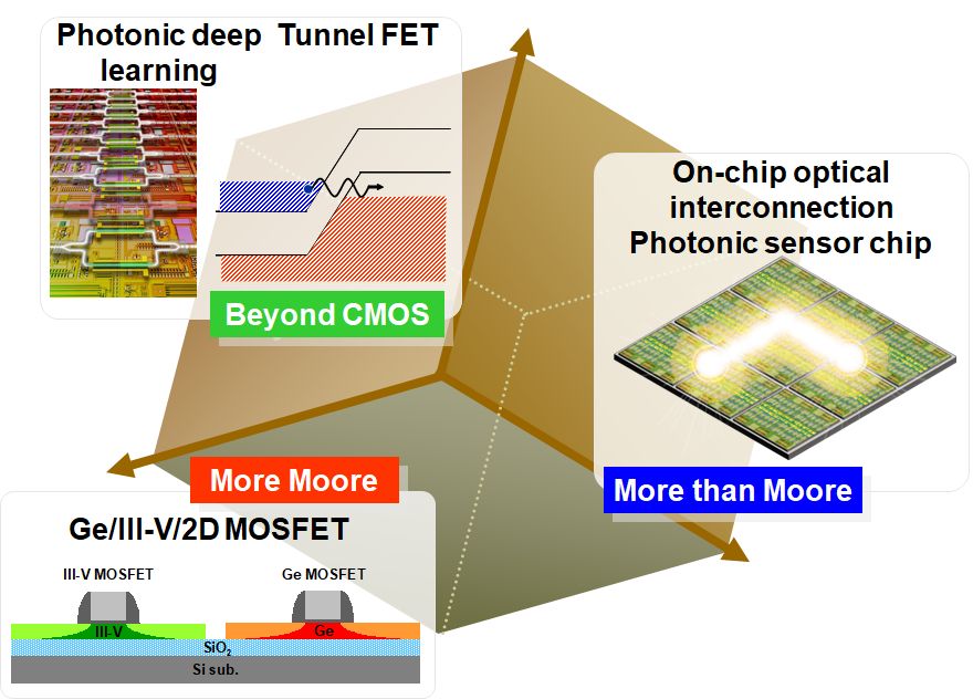
On the other hand, more computing power will be required because of the emergence of IoT and AI applications. Hence, the next-generation computing technologies has intesitvely been investigated to enhance the LSI performance without the device scaling. We are conducting researches on next-generation semiconductor devices for AI and IoT applications. Based on the heterogeneous integration of III-V semiconductors, Ge, and 2D materials on Si, we have investigated transistors and Si photonics.
As the "More Moore" approach, we have investaiged MOSFETs based on high-mobility channel materials such as III-V semicondutors and Ge. We have also investigated 2D materials for ultra-scaled MOSFETs. As the "More than Moore" approach, we have conducted the research on on-chip optical interconnect using Si photonics. Optical sensing chips based on photonics integrated circuits have also been investigated for IoT applications. As the "Beyond CMOS" approach, we are seeking new priciple for transistors including Tunnel FET and Ferroelectric FET. We have also investigated deep learning using Si photonic integrated circuits.
Main research topics: